The number of PCB layers in the chip solution of HDMI 4K video capture card, the relative position of the stack and the used board will directly affect the quality of the signal and the EMC index. The number of layers of a single board is the sum of the power layer, ground layer and signal layer. In addition, for high-speed boards, the used PCB board is also very important. Materials with a small dielectric constant must be used to improve the quality of the signal. Generally, a board with a fixed dielectric constant can be used for the inner layer.
1. Stack optimization
In practical applications, the number of layers of the board should be determined according to various factors such as the power supply of the board, the type of ground, the signal frequency, the density of signal lines, the number of signal lines required for special wiring, structural requirements, and cost control. After the number of layers is determined, the arrangement of the stacked layers in the PCB is considered. In general, the stack design should follow the following principles: Make the power plane adjacent to the ground plane.
Because the power and ground planes are equivalent to a capacitor, this capacitor will reduce the impedance of the power plane together with the decoupling capacitor on the PCB, and can also obtain a wider filtering effect. When using a multi-layer board design, you should generally try to ensure the integrity of the ground plane. Usually, it is not allowed to run signal lines on the ground plane, because that will lengthen the return path of the signal.
2. Reduce radiation
In order to improve the signal quality, it is also necessary to control the impedance of the signal lines in the board. The impedance of the single-ended signal line is mainly related to the line width, copper thickness, plate dielectric constant, and the distance between the signal line and the reference plane. The impedance of the differential signal is not only related to the above factors, but also related to the internal spacing of the differential pair. The calculation of impedance should be calculated in order according to the importance of the signal. First, plan the stack where important signal lines are located, and then perform impedance calculation. Key signals such as high-frequency, high-speed, and clock must have an adjacent complete ground plane as a reference, so as to provide a small loop area and a short return path, thereby reducing radiation.
In the PCB design stage, multiple tasks such as stack design, functional area division, impedance control, timing control, power distribution network design, and important signal isolation should be done well. In addition, the requirements of EMC and safety regulations must be fully considered to avoid a large amount of expenses caused by rectification of EMC or safety regulations in the later stage.
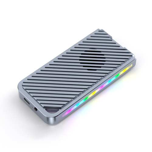
With the development of electronic technology, the increase of broadband speed and the improvement of people's living standards, people are no longer satisfied with traditional resolution images and 4K video information. The size of the family room, the size of the TV screen, personal preferences and other factors, custom resolution, so as to obtain a comfortable 4K video rendering effect, HDMI 4K video capture card chip solutionAll guarantees come from the PCB.